- 您现在的位置:买卖IC网 > Sheet目录1852 > MCP1791T-3302E/DC (Microchip Technology)IC REG LDO 3.3V 70MA SOT223-5
�� �
�
�MCP1790/MCP1791�
�1.0�
�ELECTRICAL�
�CHARACTERISTICS�
�?� Notice:� Stresses� above� those� listed� under� “Maximum� Rat-�
�ings”� may� cause� permanent� damage� to� the� device.� This� is� a�
�stress� rating� only� and� functional� operation� of� the� device� at�
�those� or� any� other� conditions� above� those� indicated� in� the�
�Absolute� Maximum� Ratings� ?�
�Input� Voltage,� V� IN� ........................................................+48.0V�
�operational� listings� of� this� specification� is� not� implied.� Expo-�
�sure� to� maximum� rating� conditions� for� extended� periods� may�
�affect� device� reliability.�
�V� IN� ,� PWRGD,� SHDN� .....................� (GND-0.3V)� to� (� V� IN� +0.3V)�
�V� OUT� ....................................................� (GND-0.3V)� to� (+5.5V)�
��Output� Short� Circuit� Current..................................Continuous�
�Storage� temperature� .....................................-55°C� to� +150°C�
��Operating� Junction� Temperature...................-40°C� to� +125°C�
�ESD� protection� on� all� pins� ........� ≥� 6� kV� HBM� and� ≥� 400V� MM�
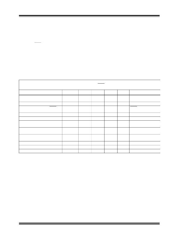
�AC/DC� CHARACTERISTICS�
�Electrical� Specifications:� Unless� otherwise� noted,� V� IN� =� V� OUT(MAX)� +� V� DROPOUT(MAX),� (Note� 1)� ,� I� OUT� =� 1� mA,�
�C� OUT� =� 4.7� μF� (X7R� Ceramic),� C� IN� =� 4.7� μF� (X7R� Ceramic),� T� A� =� +25°C,� SHDN� >� 2.4V.�
�Boldface� type� applies� for� junction� temperatures,� T� J� (Note� 5)� of� -40°C� to� +125°C.�
�Parameters�
�Input� Operating� Voltage�
�Input� Quiescent� Current�
�Input� Quiescent� Current� for� SHDN�
�Mode�
�Ground� Current�
�Maximum� Output� Current�
�Line� Regulation�
�Load� Regulation�
�Output� Peak� Short� Circuit� Current�
�Output� Voltage� Regulation�
�V� OUT� Temperature� Coefficient�
�Input� Voltage� to� Turn� On� Output�
�Symbol�
�V� IN�
�I� q�
�I� SHDN�
�I� GND�
�I� OUT�
�Δ� V� OUT� /�
�(V� OUT� X� Δ� V� IN� )�
�Δ� V� OUT� /V� OUT�
�I� OUT_SC�
�V� OUT�
�TCV� OUT�
�V� ON�
�Min�
�6.0�
�—�
�—�
�—�
�70�
�—�
�-0.45�
�—�
�V� R� -2.5%�
�—�
�—�
�Typ�
�—�
�70�
�10�
�110�
�—�
�±0.0002�
�±0.2�
�V� R� /10�
�V� R�
�65�
�5.5�
�Max�
�30.0�
�130�
�25�
�210�
�—�
�±0.05�
�0.45�
�—�
�V� R� +2.5%�
�—�
�6.0�
�Units�
�V�
�μA�
�μA�
�μA�
�mA�
�%/V�
�%�
�A�
�V�
�ppm/°C�
�V�
�Conditions�
�+48� V� DC� Load� Dump� Peak�
�<� 500� ms�
�I� L� =� 0� mA�
�SHDN� =� GND�
�I� L� =� 70� mA�
�6.0V� <� V� IN� <� 30V�
�I� OUT� =� 1� mA� to� 70� mA�
��R� LOAD� <� 0.1� � ,�
�Peak� Current�
�—�
��Rising� V� IN�
�Note� 1:�
�2:�
�3:�
�4:�
�5:�
�6:�
�7:�
�8:�
�9:�
�The� minimum� V� IN� ,� V� IN(MIN)� must� meet� two� conditions:� V� IN� ≥� 6.0� V� and� V� IN� ≥� V� OUT(MAX)� +� V� DROPOUT(MAX).�
�V� R� is� the� nominal� regulator� output� voltage.�
�Load� regulation� is� measured� at� a� constant� junction� temperature� using� low� duty� cycle� pulse� testing.� Load� regulation� is�
�tested� over� a� load� range� from� 1� mA� to� the� maximum� specified� output� current.�
�The� maximum� allowable� power� dissipation� is� a� function� of� ambient� temperature,� the� maximum� allowable� junction�
�temperature� and� the� thermal� resistance� from� junction� to� air.� (i.e.,� T� A� ,� T� J� ,� θ� JA� ).� Exceeding� the� maximum� allowable� power�
�dissipation� will� cause� the� device� operating� junction� temperature� to� exceed� the� maximum� 165°C� rating.� Sustained�
�junction� temperatures� above� 165°C� can� impact� the� device� reliability.�
�The� junction� temperature� is� approximated� by� soaking� the� device� under� test� at� an� ambient� temperature� equal� to� the�
�desired� Junction� temperature.� The� test� time� is� small� enough� such� that� the� rise� in� the� Junction� temperature� over� the�
�ambient� temperature� is� not� significant.�
�Dropout� voltage� is� defined� as� the� input-to-output� voltage� differential� at� which� the� output� voltage� drops� 2%� below� its�
�nominal� value� that� was� measured� with� an� input� voltage� of� V� IN� =� V� R� +� V� DROPOUT(� MAX� )� .�
�Sustained� junction� temperatures� above� 165°C� can� impact� the� device� reliability.�
�The� Short� Circuit� Recovery� Time� test� is� done� by� placing� the� device� into� a� short� circuit� condition� and� then� removing� the�
�short� circuit� condition� before� the� device� die� temperature� reaches� 125� °C.� If� the� device� goes� into� thermal� shutdown,� then�
�the� Short� Circuit� Recovery� Time� will� depend� upon� the� thermal� dissipation� properties� of� the� package� and� circuit� board.�
�TCV� OUT� =� (V� OUT-HIGH� -� V� OUT-LOW� )� *10^6/(V� R� *� Δ� Temperature),� V� OUT-HIGH� =� highest� voltage� measured� over� the� temperature�
�range.� V� OUT-LOW� =� lowest� voltage� measured� over� the� temperature� range.�
�DS22075B-page� 4�
�?� 2010� Microchip� Technology� Inc.�
�发布紧急采购,3分钟左右您将得到回复。
相关PDF资料
MCP1801T-1202I/OT
IC REG LDO 1.2V .15A SOT23-5
MCP1802T-1202I/OT
IC REG LDO 1.2V .26A SOT23-5
MCP1804T-A002I/DB
IC REG LDO 10V .15A SOT223-3
MCP1824ST-3002E/DB
IC REG LDO 3V .3A SOT223-3
MCP1825T-3302E/DC
IC REG LDO 3.3V .5A SOT223-5
MCP1826T-5002E/DC
IC REG LDO 5V 1A SOT223-5
MCP1827-3302E/ET
IC REG LDO 3.3V 1.5A DDPAK-5
MCP73113T-06SI/MF
IC LI-ION/LI-POLY CTRLR 10-DFN
相关代理商/技术参数
MCP1791T-3302E/DC
制造商:Microchip Technology Inc 功能描述:; Input Voltage Primary Max:30V; Output
MCP1791T-3302E/ET
功能描述:低压差稳压器 - LDO HI VLTG LDO 50 mA RoHS:否 制造商:Texas Instruments 最大输入电压:36 V 输出电压:1.4 V to 20.5 V 回动电压(最大值):307 mV 输出电流:1 A 负载调节:0.3 % 输出端数量: 输出类型:Fixed 最大工作温度:+ 125 C 安装风格:SMD/SMT 封装 / 箱体:VQFN-20
MCP1791T-5002E/DC
功能描述:低压差稳压器 - LDO HI VLTG LDO 50 mA RoHS:否 制造商:Texas Instruments 最大输入电压:36 V 输出电压:1.4 V to 20.5 V 回动电压(最大值):307 mV 输出电流:1 A 负载调节:0.3 % 输出端数量: 输出类型:Fixed 最大工作温度:+ 125 C 安装风格:SMD/SMT 封装 / 箱体:VQFN-20
MCP1791T-5002E/ET
功能描述:低压差稳压器 - LDO HI VLTG LDO 50 mA RoHS:否 制造商:Texas Instruments 最大输入电压:36 V 输出电压:1.4 V to 20.5 V 回动电压(最大值):307 mV 输出电流:1 A 负载调节:0.3 % 输出端数量: 输出类型:Fixed 最大工作温度:+ 125 C 安装风格:SMD/SMT 封装 / 箱体:VQFN-20
MCP-18
制造商:Taiyo Electric Ind. 功能描述:
MCP1801T-0902E/OT
制造商:Microchip Technology Inc 功能描述:HIGH PSRR 150 MA LDO, VIN 10V MAX, VOUT =0.9V SOT-23-5-TR - Tape and Reel
MCP1801T-0902I/OT
功能描述:低压差稳压器 - LDO Hi PSRR 150 mA LDO Vin 10V maxVout 0.9V RoHS:否 制造商:Texas Instruments 最大输入电压:36 V 输出电压:1.4 V to 20.5 V 回动电压(最大值):307 mV 输出电流:1 A 负载调节:0.3 % 输出端数量: 输出类型:Fixed 最大工作温度:+ 125 C 安装风格:SMD/SMT 封装 / 箱体:VQFN-20
MCP1801T-1202I/OT
功能描述:低压差稳压器 - LDO Hi PSRR 150 mA LDO Vin 10V maxVout 1.2V RoHS:否 制造商:Texas Instruments 最大输入电压:36 V 输出电压:1.4 V to 20.5 V 回动电压(最大值):307 mV 输出电流:1 A 负载调节:0.3 % 输出端数量: 输出类型:Fixed 最大工作温度:+ 125 C 安装风格:SMD/SMT 封装 / 箱体:VQFN-20